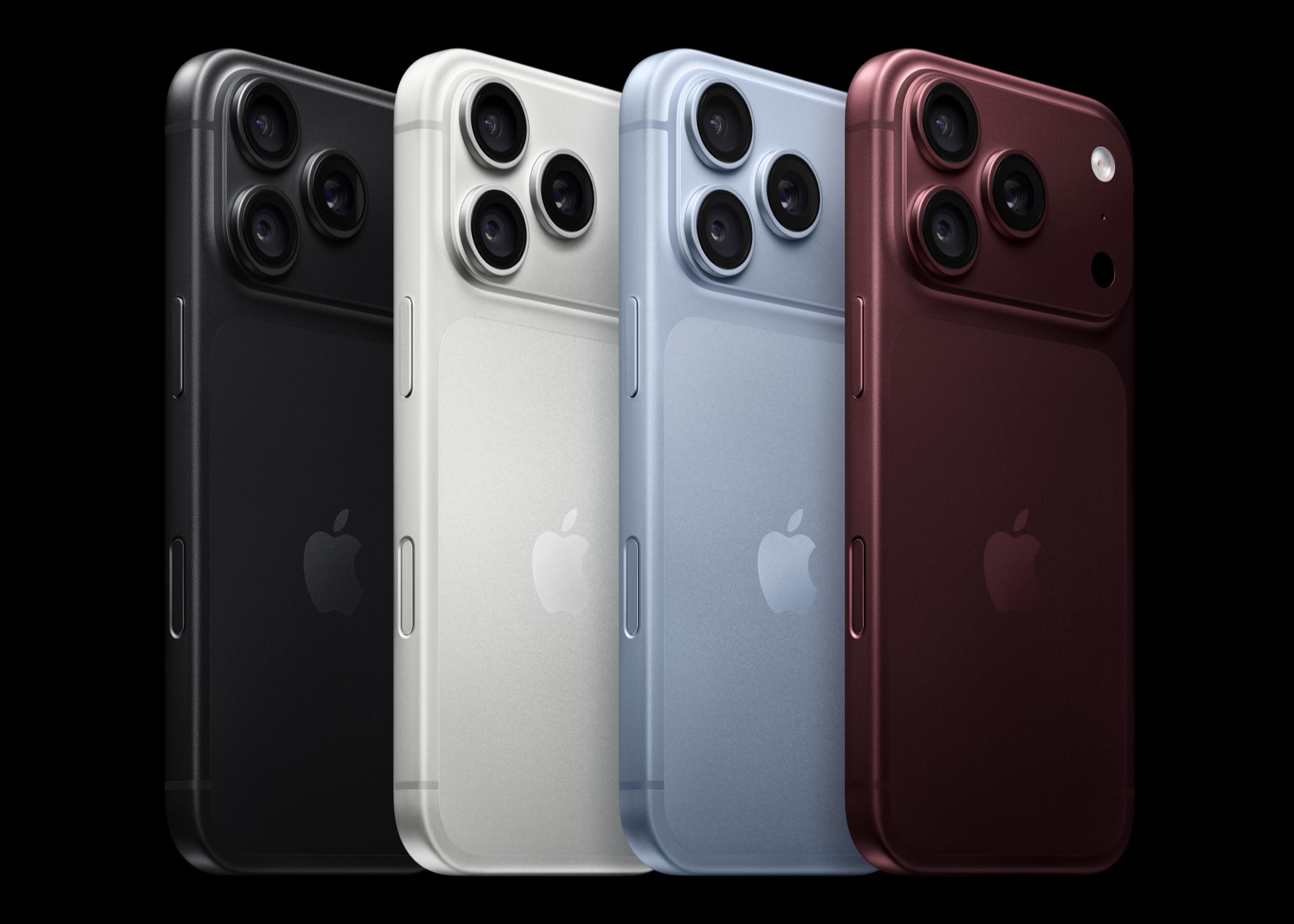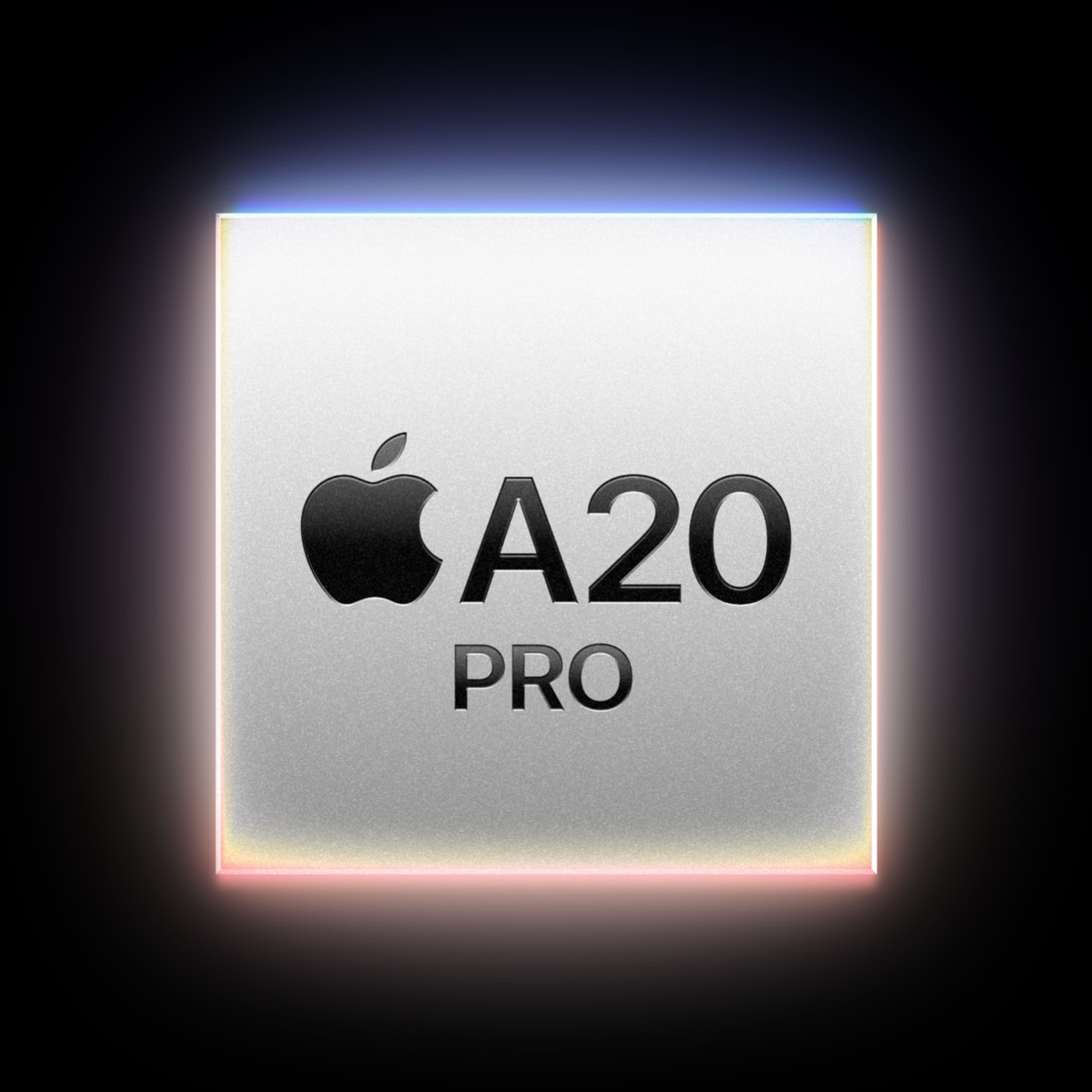
The A20 Pro in the iPhone 18 Pro is, by Apple's description, "built using the latest 2-nanometer process technology" — the first 2nm chip in a phone.
That is the headline, and it is real. It is also not the most interesting sentence in the announcement. This one is:
"A20 Pro introduces custom packaging inspired by M-series Apple silicon that places the silicon die side by side with the memory, removing the memory from the thermal path."
Almost nobody will lead with that. It is the change that makes the rest of the chip work.
What was wrong with the old arrangement
For years, iPhone processors have used a package-on-package arrangement: the DRAM sits in its own package stacked directly on top of the processor die, in the same component.
There are good reasons for it. The memory interface is as short as it can physically be, the board footprint is tiny, and in a phone both of those matter enormously.
There is one bad consequence, and it is thermal. A chip sheds heat mostly upward, through its own back. Stack memory on that back and every watt has to cross the DRAM before it reaches anything that can carry it away. Worse, DRAM is temperature-sensitive in its own right — it refreshes more often as it heats, and it has a lower ceiling than logic does. So the memory becomes both the blanket and the thermostat.
Which means the processor underneath was never really limited by the phone's cooling. It was limited by the two millimetres of memory sitting on its head.
Which is why the bigger vapor chamber is finally worth fitting
Apple also says the redesigned vapor chamber has "three times more surface area than the previous generation on iPhone 17 Pro" and "enables up to a 40 percent gain over the previous generation" in sustained performance.
Read on its own, that is a cooling upgrade. Read next to the packaging change, it is the second half of one idea.
Tripling the surface area of a heat spreader accomplishes very little if the bottleneck is between the die and the spreader rather than between the spreader and the air. Move the memory aside and the die's back is exposed for the first time — now a bigger vapor chamber has something to grip.
The datacentre-capacity piece made the same point about picking the right number: when a system has several plausible limits, the one that governs is the only one worth quoting, and it is rarely the one in the headline.
The same change pays a second time. Apple claims "50 percent more memory bandwidth than A19 Pro", from what it described at the event as the widest memory interface ever shipped in an iPhone. A stack constrains how many connections you can run between die and memory. Side by side does not, in the same way. The bandwidth and the thermal headroom come from the same decision.
Supply-chain reporting has names for the two arrangements — integrated fan-out package-on-package for the old one, wafer-level multi-chip module for the new. Those are the industry's terms, not Apple's; Apple simply says it is inspired by M-series silicon, which is accurate, because that is where side-by-side memory has lived for years.
The transistors went to AI
Set the two generations side by side and the allocation is unmistakable.
| A19 Pro | A20 Pro | |
|---|---|---|
| CPU cores | 6 | 6 |
| GPU cores | 6 | 7 |
| Neural Engine cores | 16 | 32 |
The CPU core count did not move at all. Apple's release describes "the new 6-core CPU" with "integrated Neural Accelerators", and — a small tell — compares it to "the competition" rather than to last year's chip. The generational CPU figure came at the event instead: two of the six are new supercores, about 20 percent faster, with four efficiency cores alongside.
The GPU gained a single core and Apple claims the "new 7-core GPU design is up to 40 percent faster than A19 Pro". The interesting part is not the core, it is what is in it: new Neural Accelerators with twice the FP8 throughput of the previous generation.
FP8 is an 8-bit floating-point format. Nothing renders in FP8. It exists because neural network inference tolerates low precision, and halving the bits roughly doubles what fits in memory and what crosses a bus. Apple tied it directly to running third-party large language models on the device.
And the Neural Engine doubled. Apple's wording: "a new Dual 16-core Neural Engine, which accelerates on-device AI models and computational photography, and includes 32 total cores for double the AI processing power of A19 Pro" — two blocks rather than one, addressable together by system frameworks.
So: a full node shrink, a transistor architecture change, and new packaging. The CPU core count stayed where it was, the GPU gained one, and the neural hardware doubled. Local model execution is the thing being bought, and it is being bought with essentially the entire generational budget.
What 2 nanometres actually changed
Worth being blunt: no feature on this chip is 2 nanometres. Node names stopped describing physical dimensions more than a decade ago. They are product names.
What is real about TSMC's N2 is the transistor. N2 is the company's first node built on gate-all-around nanosheet transistors, replacing the FinFET design that has been the industry standard since around 2011.
The difference is how much of the channel the gate touches. A FinFET gate wraps a vertical fin on three sides. A nanosheet gate surrounds stacked horizontal sheets on all four. More contact means better electrostatic control, which means less current leaking through when the transistor is meant to be off — the problem that has been getting steadily worse as features shrank.
TSMC's published figures for N2 against N3E: roughly 10 to 15 percent more speed at the same power, or 25 to 30 percent less power at the same speed. That is a real full-node step, and it is the first transistor-level architecture change in about fifteen years.
It is also expensive, which connects this chip to the price of the phone it sits in, though memory is doing far more of that work than the wafer is.
The 40 percent that keeps appearing
One thing worth noticing across two years of Apple's own releases:
- 2025, on A19 Pro: "up to 40 percent better sustained performance than the previous generation"
- 2026, on the vapor chamber: "enables up to a 40 percent gain over the previous generation"
- 2026, on the GPU: "up to 40 percent faster than A19 Pro"
These describe three different things, and none of them contradicts another. But taken together they suggest 40 percent has become a house figure rather than a measurement, and that "up to" is carrying its usual weight. If sustained performance genuinely rose 40 percent in each of two consecutive years, an iPhone 18 Pro would sustain roughly twice what an iPhone 16 Pro did, which is a claim nobody at Apple has made in that form.
What Apple did not say
- No transistor count. Apple stopped publishing these some generations ago.
- No RAM figure. TechInsights reads it as 12GB of LPDDR5X; Apple publishes nothing.
- No clock speeds, no die size, no cache sizes.
- No CPU comparison against A19 Pro in the written release — that number appeared only on stage.
- No independent benchmark, at time of writing, for any of it.
What is not established
- Sustained performance in independent testing. Every figure here is Apple's, against its own previous generation, under undisclosed conditions.
- How much of the thermal gain is packaging versus vapor chamber. They shipped together and Apple has not separated them.
- Yields and cost per die on N2, which bear on whether this configuration reaches non-Pro iPhones next year.
- Whether the two Neural Engine blocks can be independently allocated to different workloads, or only addressed as a pair.
- What third-party models actually run on it, at what size and speed, once developers have hardware.